Back
Next
See
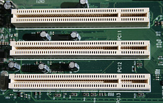
Conventional PCI
PCI/PCI-e
PCI configuration space
PCI - 1992 initial design published. Peripheral Component Interconnect
Conventional PCI
Intel creation - currently controlled by
Peripheral Component Interconnect Special Interest Group, PCI-SIG
Designed to be a CPU-neutral local bus. With right controller chip,
PCI becomes part of a CPU local/front-side bus.
Controller chip between CPU's local/front-side bus and PCI bus.
Intel and AMD make chip-sets for each of their CPUs designs.
Modern CPUs often have the PCI controller implemented on the CPU die.
Fairly fast devices interface into the PCI bus.
Second chip connects PCI to ISA bus or other slower I/O interfaces.
Evolved over a 10 year period.
On power up, operating system talks to the PCI controller using
a predefined set of memory mapped addresses.
The PCI controller then recognizes devices attached to the PCI bus.
It assigns memory addresses (ports) to each device found and coordinates
this information with the OS and device drivers.
It then acts as a memory decoder when the system addresses any device
mapped on to the bus.
Physical
Expansion ports :
 Original design - 5 volt.
Modern systems usually designed with only the 3.3 V. support.
Universal PCI systems support both in same interface.
Slots should be keyed to allow only the correct cards to be inserted.
32 bit x 33 MHz ~ 133MB/s in burst mode.
Higher performing version available in server environment.
32 bit x 66 MHz
64 bit x 33 MHz
64 bit x 66 MHz
* Also, higher throughput for 'devices' directly interfaced with
the controller (not using the physical expansion port)
62 x 2 pin connector. 2 or 4 lost to key slots.
32 bit Address/Data - multiplexed.
Also can function as either memory mapped or I/O mapped.
Non-return to zero (same as system bus).
Single-ended signaling, reflected wave.
4 interrupts.
Arranged in round robin at each expansion slot.
IRQA, slot 1 becomes IRQB, slot 2 becomes IRQC, slot3, etc.
Device can use more than one IRQ but A is first choice.
On later versions, (PCI 2.2) interrupts implemented as
message signaled interrupt (MSI).
MSI is a memory write to dedicated memory addresses set up by the
system(OS) for interrupt detection.
Software equivalent of the Programmable interrupt timer.
- Slightly longer response time.
+ Interrupts not shared between devices.
+ MSI max of 32 interrupts, MSI+ up to 2048.
4 command/byte enable (C/BE) lines.
Used in combination with !FRAME to select address or data mode.
In address mode, 4 bit command that signals type and direction of
data transfer or other command.
In data mode, masks which byte[s] to use in data transfer.
Clock line.
26 power (+3.3, +/-5, +/-12) 27 Ground
Various control/status lines.
GNT (grant), REQ (request)
- used for arbitration.
Each device/slot has its own pair.
Signals PCI controller which in turn interfaces with system.
!FRAME (frame start), IRDY (initiator ready)
- used to initiate transactions.
DEVSEL (device select), TRDY (target ready), STOP
- used by devices for status updates.
Control/status lines active low.
Only 4 devices can connect to a PCI bus but PCI buses can be
daisy chained.
* Controller is capable of controlling 256 separate buses.
Pin-out : http://www.interfacebus.com/Design_PCI_Pinout.html
Modern systems provide a single PCI slot.
Multiple PCIe ports is now the standard.
PCIe treats each device connection or expansion port as a separate bus.
Historically, most systems support 1 or 2 (bridged) PCI expansion buses.
Each bus capable of handling 4 cards (4 interrupt limitation ?)
Additional buses directly implemented on mother board to inteface
with logic such as on-board video controller.
Requires a PCI to PCI bridge to add additional items. (daisy chain)
The bridged section is treated as a separate bus.
Direct internal (on mother board) device interface usually assigned to
bus 0.
Many on-board devices/function directly wired to PCI bus 0.
Can run faster than the 33.33 MHz. - 32 device per bus addressable.
Plug and play - with support of PCI controller, system BIOS, and OS, PCI
cards auto-configure on power-up.
PCI recognizes 3 address spaces.
Main memory - maps chosen blocks main memory to be "owned" by a particular
PCI device. When addressed by drivers, PCI controller acts as decoder
for assigned memory blocks.
I/O memory - maps system i/o ports to device. Not usually used in PC
environment.
256-byte configuration memory used to discover/initialize and devices
interfacing with the PCI bus.
Devices assigned addresses, interrupts, and various memory blocks for
both control and data transfer.
Device can have up to 6 addressable blocks of 'main' memory or I/O.
Plug and Play configuration.
The CPU/OS needs to access the configuration memory to complete the PNP
implementation, i.e note/decide how memory/interrupts/DMA for a PCI
devices is allocated, etc.
It can only do this by issuing commands/requests to a specific memory port
and read/writing data to a second. These two ports, known to the system
BIOS, interface with the PCI controller which, in turn, communicates with
the configuration memory on each PCI device to complete configuration.
CPU/PCI device configuration mostly occurs at boot up.
PCI uses its own protocol for controlling/communicating with clients
devices over the configuration bus.
Controller identifies, initializes, and assigns mapped memory addresses
to discovered PCI cards, chips, and devices.
Uses 16 bit address structure :
8-bit configuration space ID(bus) - 256 separate buses.
5-bit device ID - 32 devices.
3-bit function ID (BDF) - up to 8 addressable functions per device.
When system 1st comes up, it requests an 'enumeration' of the
PCI bus - it asks the PCI controller to find out what is connected.
PCI cards contain information that allows system to correctly interface
to them. Function 0 of any device must exist and return the card's
device and vendor ids when contacted by controller.
PCI cards can contain executable code that activates them before the OS
and software drivers are loaded.
Each device has a 256 byte area that the controller can contact when
in configuration mode. The controller sequences through each bus
and device id and attempts to invoke function 0.
If a device is connected, function 0 will return information and
the controller will negotiate an initial memory @ ranges
or i/o ports on the system bus.
If no device exists, then there is no function 0 and the controller
moves on to the next bus/device address.
Discovered devices are informed of the addresses assigned to them.
PCI uses multiplexing to optimize use of pin-out on cards. It uses the same
pins for address, data, and device specific control.
If correctly configured, devices will recognize when they are being
addressed via memory / I/O mapped addresses.
*******
Conventional PCI uses the 32 bit address/data line set and 4 bit command/mask
line set to indicate memory space, specific address, and direction of
transaction, and type of transaction.
Conventional PCI uses a transaction based communication.
A command is issued indicating the type of transaction being performed,
Read, Write, burst read or write, message signaled interrupt, etc.
Additional information applied to data lines.
This may be followed by a series of data transfers (0 to many).
Initiator or target eventually terminates transation for a variety of
reasons.
The combination of address/data/control lines with other control lines
on the interface allows to PCI to specify task and addressing information
and then transfer large blocks of data between system and device,
usually without the intervention of the CPU after initialization.
Transmitting data
Original design - 5 volt.
Modern systems usually designed with only the 3.3 V. support.
Universal PCI systems support both in same interface.
Slots should be keyed to allow only the correct cards to be inserted.
32 bit x 33 MHz ~ 133MB/s in burst mode.
Higher performing version available in server environment.
32 bit x 66 MHz
64 bit x 33 MHz
64 bit x 66 MHz
* Also, higher throughput for 'devices' directly interfaced with
the controller (not using the physical expansion port)
62 x 2 pin connector. 2 or 4 lost to key slots.
32 bit Address/Data - multiplexed.
Also can function as either memory mapped or I/O mapped.
Non-return to zero (same as system bus).
Single-ended signaling, reflected wave.
4 interrupts.
Arranged in round robin at each expansion slot.
IRQA, slot 1 becomes IRQB, slot 2 becomes IRQC, slot3, etc.
Device can use more than one IRQ but A is first choice.
On later versions, (PCI 2.2) interrupts implemented as
message signaled interrupt (MSI).
MSI is a memory write to dedicated memory addresses set up by the
system(OS) for interrupt detection.
Software equivalent of the Programmable interrupt timer.
- Slightly longer response time.
+ Interrupts not shared between devices.
+ MSI max of 32 interrupts, MSI+ up to 2048.
4 command/byte enable (C/BE) lines.
Used in combination with !FRAME to select address or data mode.
In address mode, 4 bit command that signals type and direction of
data transfer or other command.
In data mode, masks which byte[s] to use in data transfer.
Clock line.
26 power (+3.3, +/-5, +/-12) 27 Ground
Various control/status lines.
GNT (grant), REQ (request)
- used for arbitration.
Each device/slot has its own pair.
Signals PCI controller which in turn interfaces with system.
!FRAME (frame start), IRDY (initiator ready)
- used to initiate transactions.
DEVSEL (device select), TRDY (target ready), STOP
- used by devices for status updates.
Control/status lines active low.
Only 4 devices can connect to a PCI bus but PCI buses can be
daisy chained.
* Controller is capable of controlling 256 separate buses.
Pin-out : http://www.interfacebus.com/Design_PCI_Pinout.html
Modern systems provide a single PCI slot.
Multiple PCIe ports is now the standard.
PCIe treats each device connection or expansion port as a separate bus.
Historically, most systems support 1 or 2 (bridged) PCI expansion buses.
Each bus capable of handling 4 cards (4 interrupt limitation ?)
Additional buses directly implemented on mother board to inteface
with logic such as on-board video controller.
Requires a PCI to PCI bridge to add additional items. (daisy chain)
The bridged section is treated as a separate bus.
Direct internal (on mother board) device interface usually assigned to
bus 0.
Many on-board devices/function directly wired to PCI bus 0.
Can run faster than the 33.33 MHz. - 32 device per bus addressable.
Plug and play - with support of PCI controller, system BIOS, and OS, PCI
cards auto-configure on power-up.
PCI recognizes 3 address spaces.
Main memory - maps chosen blocks main memory to be "owned" by a particular
PCI device. When addressed by drivers, PCI controller acts as decoder
for assigned memory blocks.
I/O memory - maps system i/o ports to device. Not usually used in PC
environment.
256-byte configuration memory used to discover/initialize and devices
interfacing with the PCI bus.
Devices assigned addresses, interrupts, and various memory blocks for
both control and data transfer.
Device can have up to 6 addressable blocks of 'main' memory or I/O.
Plug and Play configuration.
The CPU/OS needs to access the configuration memory to complete the PNP
implementation, i.e note/decide how memory/interrupts/DMA for a PCI
devices is allocated, etc.
It can only do this by issuing commands/requests to a specific memory port
and read/writing data to a second. These two ports, known to the system
BIOS, interface with the PCI controller which, in turn, communicates with
the configuration memory on each PCI device to complete configuration.
CPU/PCI device configuration mostly occurs at boot up.
PCI uses its own protocol for controlling/communicating with clients
devices over the configuration bus.
Controller identifies, initializes, and assigns mapped memory addresses
to discovered PCI cards, chips, and devices.
Uses 16 bit address structure :
8-bit configuration space ID(bus) - 256 separate buses.
5-bit device ID - 32 devices.
3-bit function ID (BDF) - up to 8 addressable functions per device.
When system 1st comes up, it requests an 'enumeration' of the
PCI bus - it asks the PCI controller to find out what is connected.
PCI cards contain information that allows system to correctly interface
to them. Function 0 of any device must exist and return the card's
device and vendor ids when contacted by controller.
PCI cards can contain executable code that activates them before the OS
and software drivers are loaded.
Each device has a 256 byte area that the controller can contact when
in configuration mode. The controller sequences through each bus
and device id and attempts to invoke function 0.
If a device is connected, function 0 will return information and
the controller will negotiate an initial memory @ ranges
or i/o ports on the system bus.
If no device exists, then there is no function 0 and the controller
moves on to the next bus/device address.
Discovered devices are informed of the addresses assigned to them.
PCI uses multiplexing to optimize use of pin-out on cards. It uses the same
pins for address, data, and device specific control.
If correctly configured, devices will recognize when they are being
addressed via memory / I/O mapped addresses.
*******
Conventional PCI uses the 32 bit address/data line set and 4 bit command/mask
line set to indicate memory space, specific address, and direction of
transaction, and type of transaction.
Conventional PCI uses a transaction based communication.
A command is issued indicating the type of transaction being performed,
Read, Write, burst read or write, message signaled interrupt, etc.
Additional information applied to data lines.
This may be followed by a series of data transfers (0 to many).
Initiator or target eventually terminates transation for a variety of
reasons.
The combination of address/data/control lines with other control lines
on the interface allows to PCI to specify task and addressing information
and then transfer large blocks of data between system and device,
usually without the intervention of the CPU after initialization.
Transmitting data