Dynamic Random Access memory
Capacitor based bit storage.
Laid out in rectangular grids.
Rows and columns.
Each grid represents 1 bit of a byte or word on a chip.
A bank of chips provide the byte or word.
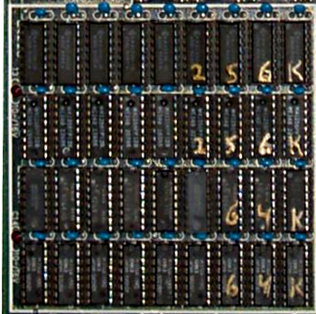 SDRAM arranged so that 1 to 4 bits of a byte stored on a chip.
Multiple chips placed on a circuit board module.
This allowed for a particular chip to have a fewer number of pins.
SDRAM arranged so that 1 to 4 bits of a byte stored on a chip.
Multiple chips placed on a circuit board module.
This allowed for a particular chip to have a fewer number of pins.
 Target address split into row and column address by a memory controller.
This allows for a smaller number of pins to address the memory.
But requires additional control circuitry and extra clock cycle to
specify full address.
Early memory was often asynchronous - it did not perform in time
with the system/bus clock.
The memory controller was responsible for synchronizing data transfers.
Memory chip has a small bank of static ram gates/sense amplifiers that
function both to boost the signal of a cell and to amplify current
state of a row for refresh write-back.
For the 64Kib chip below, this would be a 256 byte sense amp line.
2^8 (256) rows by 2^8 (256) columns.
Readings :
arstechnica.com/paedia/r/ram_guide/ram_guide.part1-1.html
arstechnica.com/paedia/r/ram_guide/ram_guide.part2-1.html
arstechnica.com/paedia/r/ram_guide/ram_guide.part3-1.html
https://people.freebsd.org/~lstewart/articles/cpumemory.pdf
4164 - 64kx1 DRAM.
# /RAS and /CAS also function as a substitute for a CE (chip enable).
i.e if both are held high, Din and Dout are tri-state (disconnected)
and any input on the address and Din pins is ignored.
Target address split into row and column address by a memory controller.
This allows for a smaller number of pins to address the memory.
But requires additional control circuitry and extra clock cycle to
specify full address.
Early memory was often asynchronous - it did not perform in time
with the system/bus clock.
The memory controller was responsible for synchronizing data transfers.
Memory chip has a small bank of static ram gates/sense amplifiers that
function both to boost the signal of a cell and to amplify current
state of a row for refresh write-back.
For the 64Kib chip below, this would be a 256 byte sense amp line.
2^8 (256) rows by 2^8 (256) columns.
Readings :
arstechnica.com/paedia/r/ram_guide/ram_guide.part1-1.html
arstechnica.com/paedia/r/ram_guide/ram_guide.part2-1.html
arstechnica.com/paedia/r/ram_guide/ram_guide.part3-1.html
https://people.freebsd.org/~lstewart/articles/cpumemory.pdf
4164 - 64kx1 DRAM.
# /RAS and /CAS also function as a substitute for a CE (chip enable).
i.e if both are held high, Din and Dout are tri-state (disconnected)
and any input on the address and Din pins is ignored.
 Early systems used a bank of 8 or 9 1 bit DIP packages. Signals sent to all
chips in parallel and data i/o pins were wired to the proper data line.
Newer RAM modules do this stacking internally.
When memory is accessed, the request is usually passed to memory controller.
* Memory address pins not directly connected to the system bus.
Memory address pins multiplexed
- takes high (row) then low (column) halves of address sequentially.
(Original design).
To read a memory cell
The controller takes the address and splits it into row and column addresses.
It also handles timing response delays (waits) while the rows and columns
are strobed onto the memory itself and the memory responds.
While this is happening, memory control circuit is signaling CPU to 'wait'
if needed.
While RAS held high (row address select)
Row address of memory supplied to A0-Ax
!RAS brought low and !CAS held high latching the high half of @ or row.
!WE held high indicating a read.
Column address supplied to A0-Ax
!CAS brought low latching the low half of @ or column.
Once cell has time to respond
Data should appear on Data line
At this point !CAS brought back high
Followed by !RAS being brought back high indicating end of read cycle.
(This also isolates data i/o from bus.)
For write, !WE brought low brought at appropriate time and data
transferred into the cell.
On chips that use OE (output enable), the memory controller would have
also toggle appropriate signal.
Basic Dynamic Random Access Memory (Re)ram
C64 memory access schematic
XT mother board
PCI mother board
DRAM timing
Early systems used a bank of 8 or 9 1 bit DIP packages. Signals sent to all
chips in parallel and data i/o pins were wired to the proper data line.
Newer RAM modules do this stacking internally.
When memory is accessed, the request is usually passed to memory controller.
* Memory address pins not directly connected to the system bus.
Memory address pins multiplexed
- takes high (row) then low (column) halves of address sequentially.
(Original design).
To read a memory cell
The controller takes the address and splits it into row and column addresses.
It also handles timing response delays (waits) while the rows and columns
are strobed onto the memory itself and the memory responds.
While this is happening, memory control circuit is signaling CPU to 'wait'
if needed.
While RAS held high (row address select)
Row address of memory supplied to A0-Ax
!RAS brought low and !CAS held high latching the high half of @ or row.
!WE held high indicating a read.
Column address supplied to A0-Ax
!CAS brought low latching the low half of @ or column.
Once cell has time to respond
Data should appear on Data line
At this point !CAS brought back high
Followed by !RAS being brought back high indicating end of read cycle.
(This also isolates data i/o from bus.)
For write, !WE brought low brought at appropriate time and data
transferred into the cell.
On chips that use OE (output enable), the memory controller would have
also toggle appropriate signal.
Basic Dynamic Random Access Memory (Re)ram
C64 memory access schematic
XT mother board
PCI mother board
DRAM timing