Lectures
Read : https://en.wikipedia.org/wiki/Flip-flop_(electronics)
Memory units - Latches.
Hysteresis - time based system that is dependent on its internal state or
previous condition.
A memory unit must not only toggle to the value specified, it
must hold that value after the initial set condition expired.
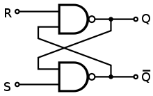
a. SR Latch
i. Set - Reset
ii. Pair of NOR or NAND gates that feed back to each other.
iii. Level driven.
iv. On NOR latch, 1 1 is considered an invalid input.
On NAND latch, 0 0 is considered an invalid input.
Synchronous Logic
The main advantage of synchronous logic is its simplicity. The logic gates which perform the operations on the data require a finite amount of time to respond to changes to their inputs. This is called propagation delay. The interval between clock pulses must be long enough so that all the logic gates have time to respond to the changes and their outputs "settle" to stable logic values, before the next clock pulse occurs. As long as this condition is met (ignoring certain other details) the circuit is guaranteed to be stable and reliable.
From wikipedia topic Sequential Logic
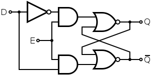
Clocked D latch
a. Clocked D latch
i. SR replaced with a single input (the data).
ii. 1 bit memory.
iii. Allows changes when E is high.
iv. Holds setting when E is low.
Depending on use, E is either a write enable, a clock signal, or both.
Clock signals signals divide time up into 2 periods.
During the enable period, gate accepts new input for next state.
* Logic assumes input is stable.
During the other, gate processes previously accepted input,
adjusting data on output lines,
and ignores any further change on input lines.
 source
| Data | Enable | Q |
| 0 | 0 | Hold |
| 1 | 0 | Hold |
| 0 | 1 | 0 |
| 1 | 1 | 1 |
 By Marble machine - Own work, CC BY-SA 4.0, https://commons.wikimedia.org/w/index.php?curid=48013320
"Dark" bit = 1, "Light" bit = 0
In a practical memory data latch,
!Q would be inverted and combined with Q which would be relabeled Dout.
Memory units - flip-flops
https://en.wikipedia.org/wiki/Flip-flop_%28electronics%29
a. Latches are level triggered.
Write enable (trigger) held high for 1/2 length of clock.
b. Flip-flops are 'edge' sensitive or triggered.
i. Data latched when clock changes.
ii. Can be designed to trigger on rising Or falling edge.
iii. Actually, a very short period level trigger.
iv. Allows more time for circuit to process input.
By Marble machine - Own work, CC BY-SA 4.0, https://commons.wikimedia.org/w/index.php?curid=48013320
"Dark" bit = 1, "Light" bit = 0
In a practical memory data latch,
!Q would be inverted and combined with Q which would be relabeled Dout.
Memory units - flip-flops
https://en.wikipedia.org/wiki/Flip-flop_%28electronics%29
a. Latches are level triggered.
Write enable (trigger) held high for 1/2 length of clock.
b. Flip-flops are 'edge' sensitive or triggered.
i. Data latched when clock changes.
ii. Can be designed to trigger on rising Or falling edge.
iii. Actually, a very short period level trigger.
iv. Allows more time for circuit to process input.
 c. Propagation delay -
time needed for a sequence of circuits to change to a new state.
d. Using propagation delays and cancellation to create a edge pulse.
c. Propagation delay -
time needed for a sequence of circuits to change to a new state.
d. Using propagation delays and cancellation to create a edge pulse.
 Memory bank
Alternative memory cell to flip-flops - dynamic ram.
Memory chips built with CMOS flip-flops are very power-efficient and fast,
but require 4-6 transistors per bit.
DRAM uses a single transistor/capacitor pair per bit.
+ Much smaller foot-print
- But require periodic scheduled refreshing
- Reads destructive, require re-writing of data.
Read : https://en.wikipedia.org/wiki/Dynamic_random-access_memory sections 1-4
Memory bank
Alternative memory cell to flip-flops - dynamic ram.
Memory chips built with CMOS flip-flops are very power-efficient and fast,
but require 4-6 transistors per bit.
DRAM uses a single transistor/capacitor pair per bit.
+ Much smaller foot-print
- But require periodic scheduled refreshing
- Reads destructive, require re-writing of data.
Read : https://en.wikipedia.org/wiki/Dynamic_random-access_memory sections 1-4

 Source

 Source