Back
Lecture
Current Flash memory.
Flash memory
Sourced from www.omicsonline.org - a site that makes Creative Commons
licensed publications available.
https://www.omicsonline.org/open-access/nand-flash-memory-organization-and-operations-2165-7866-1000139.pdf
Also https://www.explainthatstuff.com/flashmemory.html
A form of EEPROM with some significant differences.
Uses different physics from EEPROMs to set or clear bits but
effect same - charging or discharging floating gate.

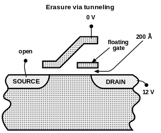 A gate consists of
floating gate (fg) - an isolated part of the cell that can be set or cleared
of electrons.
If charged, actually set bit to 0. (turns off transistor).
control gate (cg) - used to sense setting on floating gate
or to set or clear floating gate.
For read, control gate is charged to half way (+) between the charge of a
set floating gate and a cleared floating gate.
If floating gate is charged, the control gate's charge is too weak to
over-ride the floating gate and the bit transistor still signals 0.
If floating gate is uncharged, the control gate's charge causes the bit
transistor to signal a 1.
Setting and clearing of floating gate are performed by applying higher/lower
than normal voltages on the control gate, drain, and source.
Two logic architectures, NOR and NAND. Each offers different features.
For purpose of erasing/resetting,
memory erase at block level, required for NAND, available for NOR.
Separate circuit called a charge pump generates required voltage.
NOR :
A gate consists of
floating gate (fg) - an isolated part of the cell that can be set or cleared
of electrons.
If charged, actually set bit to 0. (turns off transistor).
control gate (cg) - used to sense setting on floating gate
or to set or clear floating gate.
For read, control gate is charged to half way (+) between the charge of a
set floating gate and a cleared floating gate.
If floating gate is charged, the control gate's charge is too weak to
over-ride the floating gate and the bit transistor still signals 0.
If floating gate is uncharged, the control gate's charge causes the bit
transistor to signal a 1.
Setting and clearing of floating gate are performed by applying higher/lower
than normal voltages on the control gate, drain, and source.
Two logic architectures, NOR and NAND. Each offers different features.
For purpose of erasing/resetting,
memory erase at block level, required for NAND, available for NOR.
Separate circuit called a charge pump generates required voltage.
NOR :
 A byte consists of 8 separate (parallel) bit lines.
Byte addressable read.
Memory mapped.
Default (erased) bits set to 1. Setting a bit zeros it.
Slow erase/write times.
Individual byte has to be erased before writing new byte value.
x10 slower than NAND to erase/write.
Block erase commonly implemented on modern NOR to improve write
performance. Block erase time same as byte erase.
Faster read than NAND but slower that other ROMs and SRAM (flip-flop).
Used for directly executable code (byte readable).
Limited number of changes possible but used where this is not
an issue. 10x to 100,000x (for $).
Used in modern computer BIOS-es.
Because of byte level access,
Made to higher specifications (cost+).
Larger 'real estate' to address each byte (lower density).
When accessed at byte level, requires sufficient address lines and
multiple bit lines.
Generally used instead of EEPROM on most modern systems.
NAND :
Arranged as row of AND-ed bits.
Behaves like other 2ndardy memory,
data read and written serially in blocks.
A byte consists of 8 separate (parallel) bit lines.
Byte addressable read.
Memory mapped.
Default (erased) bits set to 1. Setting a bit zeros it.
Slow erase/write times.
Individual byte has to be erased before writing new byte value.
x10 slower than NAND to erase/write.
Block erase commonly implemented on modern NOR to improve write
performance. Block erase time same as byte erase.
Faster read than NAND but slower that other ROMs and SRAM (flip-flop).
Used for directly executable code (byte readable).
Limited number of changes possible but used where this is not
an issue. 10x to 100,000x (for $).
Used in modern computer BIOS-es.
Because of byte level access,
Made to higher specifications (cost+).
Larger 'real estate' to address each byte (lower density).
When accessed at byte level, requires sufficient address lines and
multiple bit lines.
Generally used instead of EEPROM on most modern systems.
NAND :
Arranged as row of AND-ed bits.
Behaves like other 2ndardy memory,
data read and written serially in blocks.
 By wikipedia user Cyferz, CC BY-SA 3.0
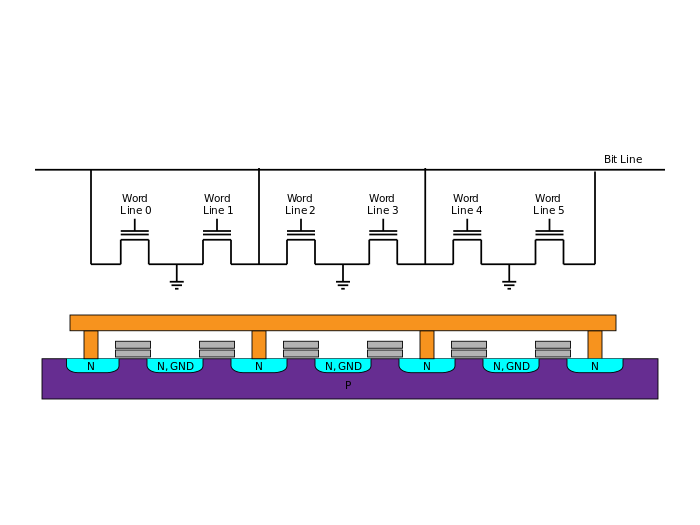
To read :
Bit line select transistor is turned on.
Most of the word lines (control gates) are set to just above a set bit.
Not enough to alter the floating gate.
But making it look like all the bits are set.
The targeted word line control gate is set to just above an erased bit.
If a word line floating gate is set,
charge on control gate is canceled and bit line stays high.
If a word line floating gate is erased,
charge on the control gate will bring the bit line low.
Controller then strobes through each AND-ed word line,
outputting the bit of all AND-ed words serially.
Because the controller knows which word it is addressing as it strobes,
it know the source of bit being read out.
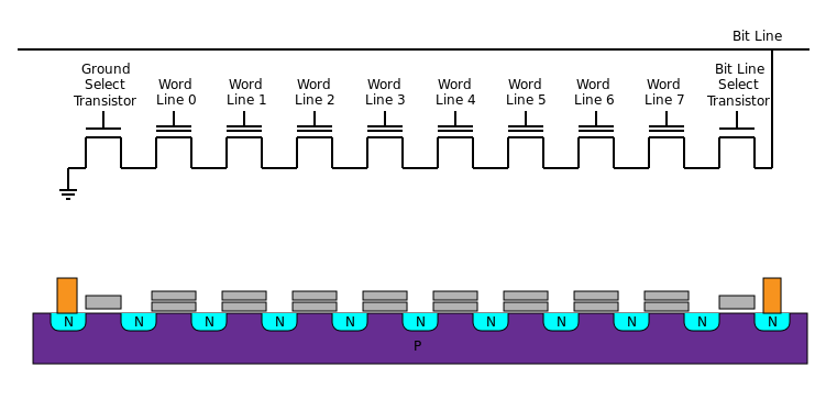
# separate bit lines for each bit of the byte/word.
see https://www.omicsonline.org/open-access/nand-flash-memory-organization-and-operations-2165-7866-1000139.pdf
Data organized in page/block units and read by page
and written/erased by block.
Page of memory read by sequencing the word line control gates of
a particular row.
Block written sequentially.
This is the result both the nature of NAND design and to reduce costs.
Page of 512, 2048, or 4096 bytes + error correcting bytes.
Block size :
32 x 512 byte pages, 64 x 2048 byte pages, 128 x 4096 byte pages.
Faster write/erase than NOR but slower than RAM.
10s of times more durable than NOR. (Generally guaranteed for 1,000,000 )
Part of this is accomplished by wear distribution and the ability of the
chip to note and hide bad blocks, especially in the NAND form.
Behaves and is implemented as secondary rather than primary storage.
Flash memory (Thumb Drive, memory stick, Jump-Drive)
and SSD (solid-state hard drives)
Check out thessdguy.com
Used anywhere sequential read/writes practical.
Not useful for BIOS or extra "primary memory"
NAND flash transistors are often smaller than ideally needed to create
a reliable gate and a number of them are often bad from the start.
SSDs use higher quality gates. You also pay more.
Better quality.
Uses error correcting code - requiring additional bits.
Many spare blocks for wear and bad block replacement.
Most flash ROMs come with bad blocks that have been flagged from start.
Allowing for cheaper manufacturing.
Magnetic drive manufacturers use similar practice on hard drives.
Flash stick (thumb drives) consist of a NAND ROM chip and a controller
chip.
Driver on the PC addresses the controller not the ROM.
The controller then addresses the ROM and handles sequencing through
an addressed words on a target bit line.
USB2 is capable of about 40MB/sec.
Newer SSD drives support USB 3 with 650MB/sec.
Some newer implementations of Flash ROM support multiple charge levels.
* 4 charge level or state cell acts as a 2-bit cell.
* 8 state or 3-bit cell exists, used in some SSD drives.
Multi-level cells require more advanced error checking.
Makes writing trickier.
Provides more storage without increasing the number of cells.
SSD - have advanced controllers and can access banks of chips in parallel
giving providing read access of up to 600MiB/sec (SATA).
2019 Spring
500GB $67
1TB $130 vs 1TB HD $40
USB stick size and OS file-systems.
FAT-32 (File allocation table)
Smaller USB sticks use/used FAT32.
Universally readable/writable by most systems.
Maximum file size 4GiB,
Maximum file count 64KB per directory.
File block/cluster size as large as 64KiB (2^18)
even if file is 2 bytes long.
ExFAT
Maximum file size 128 PiB (2^50),
Maximum file count 2796202 per directory.
Permits even large block/cluster sizes.
NTFS
Much better storage allocation
But Microsoft proprietary.
Other OSes may not be able to read or write to.
UDF - universal disk format is usable by most modern OSes and
supports larger USB drives and larger files (> 4GB).
Generally universal
but has a fair number of revisions.
Various Unix formats, supported by OSX and Linux but not by MS.
By wikipedia user Cyferz, CC BY-SA 3.0
To read :
Bit line select transistor is turned on.
Most of the word lines (control gates) are set to just above a set bit.
Not enough to alter the floating gate.
But making it look like all the bits are set.
The targeted word line control gate is set to just above an erased bit.
If a word line floating gate is set,
charge on control gate is canceled and bit line stays high.
If a word line floating gate is erased,
charge on the control gate will bring the bit line low.
Controller then strobes through each AND-ed word line,
outputting the bit of all AND-ed words serially.
Because the controller knows which word it is addressing as it strobes,
it know the source of bit being read out.
# separate bit lines for each bit of the byte/word.
see https://www.omicsonline.org/open-access/nand-flash-memory-organization-and-operations-2165-7866-1000139.pdf
Data organized in page/block units and read by page
and written/erased by block.
Page of memory read by sequencing the word line control gates of
a particular row.
Block written sequentially.
This is the result both the nature of NAND design and to reduce costs.
Page of 512, 2048, or 4096 bytes + error correcting bytes.
Block size :
32 x 512 byte pages, 64 x 2048 byte pages, 128 x 4096 byte pages.
Faster write/erase than NOR but slower than RAM.
10s of times more durable than NOR. (Generally guaranteed for 1,000,000 )
Part of this is accomplished by wear distribution and the ability of the
chip to note and hide bad blocks, especially in the NAND form.
Behaves and is implemented as secondary rather than primary storage.
Flash memory (Thumb Drive, memory stick, Jump-Drive)
and SSD (solid-state hard drives)
Check out thessdguy.com
Used anywhere sequential read/writes practical.
Not useful for BIOS or extra "primary memory"
NAND flash transistors are often smaller than ideally needed to create
a reliable gate and a number of them are often bad from the start.
SSDs use higher quality gates. You also pay more.
Better quality.
Uses error correcting code - requiring additional bits.
Many spare blocks for wear and bad block replacement.
Most flash ROMs come with bad blocks that have been flagged from start.
Allowing for cheaper manufacturing.
Magnetic drive manufacturers use similar practice on hard drives.
Flash stick (thumb drives) consist of a NAND ROM chip and a controller
chip.
Driver on the PC addresses the controller not the ROM.
The controller then addresses the ROM and handles sequencing through
an addressed words on a target bit line.
USB2 is capable of about 40MB/sec.
Newer SSD drives support USB 3 with 650MB/sec.
Some newer implementations of Flash ROM support multiple charge levels.
* 4 charge level or state cell acts as a 2-bit cell.
* 8 state or 3-bit cell exists, used in some SSD drives.
Multi-level cells require more advanced error checking.
Makes writing trickier.
Provides more storage without increasing the number of cells.
SSD - have advanced controllers and can access banks of chips in parallel
giving providing read access of up to 600MiB/sec (SATA).
2019 Spring
500GB $67
1TB $130 vs 1TB HD $40
USB stick size and OS file-systems.
FAT-32 (File allocation table)
Smaller USB sticks use/used FAT32.
Universally readable/writable by most systems.
Maximum file size 4GiB,
Maximum file count 64KB per directory.
File block/cluster size as large as 64KiB (2^18)
even if file is 2 bytes long.
ExFAT
Maximum file size 128 PiB (2^50),
Maximum file count 2796202 per directory.
Permits even large block/cluster sizes.
NTFS
Much better storage allocation
But Microsoft proprietary.
Other OSes may not be able to read or write to.
UDF - universal disk format is usable by most modern OSes and
supports larger USB drives and larger files (> 4GB).
Generally universal
but has a fair number of revisions.
Various Unix formats, supported by OSX and Linux but not by MS.